
Fișier:Wafer flats convention v2.svg

Mărește rezoluția imaginii (Fișier SVG, cu dimensiunea nominală de 150 × 150 pixeli, mărime fișier: 13 KB)
| Acest fișier se află la Wikimedia Commons. Consultați pagina sa descriptivă acolo. |
Descriere fișier
| Descriere |
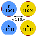
Wafer flats convention, based on Image:Wafer flats convention.PNG Conventional meaning of flats in semiconductor wafers. Red denotes material that has been removed. Wafer orientation is the orientation of the crystallographic plane in which the crystal grew. Wafer type indicated the type of doping.
|
| Dată | |
| Sursă |
self-made, Această imagine vectorială a fost creată cu Inkscape . |
| Autor | Twisp |
| Alte versiuni | Wafer flats convention.PNG |
Licențiere
| Eu, deținătorul drepturilor de autor ale acestei opere, o eliberez domeniului public. Aceasta se aplică în întreaga lume. În anumite țări există posibilitatea ca acest lucru să nu fie legal posibil; în acest caz: permit oricui să utilizeze această operă în orice scop, fără nicio condiție, atâta timp cât asemenea condiții nu sunt cerute de lege. |
Istoricul fișierului
Apăsați pe Data și ora pentru a vedea versiunea trimisă atunci.
| Data și ora | Miniatură | Dimensiuni | Utilizator | Comentariu | |
|---|---|---|---|---|---|
| actuală | 25 septembrie 2013 00:40 | | 150x150 (13 KB) | Cepheiden | fixed position of secondary flat Silicon processing for the VLSI era - Vol. 1 - Process technology; S Wolf; RN Tauber - Lattice Press; 1986; ISBN 096167237; p. 23 |
| 23 decembrie 2008 03:37 |  | 150x150 (13 KB) | Inductiveload | Added arrow indication <110> direction and enlarged flats so they can be easily seen | |
| 1 martie 2008 00:17 |  | 150x150 (9 KB) | Twisp | ||
| 1 martie 2008 00:13 |  | 150x150 (9 KB) | Twisp | ||
| 1 martie 2008 00:06 |  | 150x150 (8 KB) | Twisp | ||
| 29 februarie 2008 23:59 |  | 150x150 (8 KB) | Twisp | ||
| 29 februarie 2008 21:09 |  | 150x150 (9 KB) | Twisp | {{Information |Description= Wafer flats convention, based on Image:Wafer flats convention.PNG Conventional meaning of ''flats'' in semiconductor wafers. Black denotes material that has been removed. Wafer orientation is |
Utilizarea fișierului
Următoarele pagini conțin această imagine:
Utilizarea globală a fișierului
Următoarele alte proiecte wiki folosesc acest fișier:
- Utilizare la ca.wikipedia.org
- Utilizare la cs.wikipedia.org
- Utilizare la de.wikipedia.org
- Utilizare la en.wikipedia.org
- Utilizare la es.wikipedia.org
- Utilizare la et.wikipedia.org
- Utilizare la eu.wikipedia.org
- Utilizare la fi.wikipedia.org
- Utilizare la it.wikipedia.org
- Utilizare la it.wikibooks.org
- Utilizare la ja.wikipedia.org
- Utilizare la ko.wikipedia.org
- Utilizare la nl.wikipedia.org
- Utilizare la pl.wikipedia.org
- Utilizare la sk.wikipedia.org
- Utilizare la uk.wikipedia.org
- Utilizare la www.wikidata.org